Contract Manufacturing
Circuit Card Assembly (CCA)
Accelerate Mission Success with Spirit's High-Reliability CCA Solutions.
As a trusted, AS9100-certified U.S. partner, Spirit eliminates multi-vendor complexity through complete supply chain integration—from authorized component sourcing, part modifications, advanced up-screening to final system testing—delivering superior quality, counterfeit prevention, and faster time-to-market for your mission-critical applications.
Other Common Names:
Surface Mount Technology (SMT) Assembly, Printed Circuit Board Assembly (PCBA), Printed Wiring Assembly (PWA), PCB Assembly, Printed Wiring Board (PWB)
Features & Capabilities
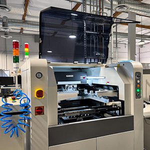
Advanced Circuit Card Assembly
Rapid Development & Prototyping
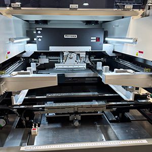
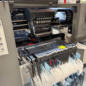
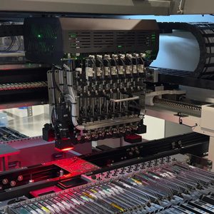
- Advanced Automated SMT Assembly
- Prototype and 1st Time Builds
- Small Lot Friendly
- PCB Design and Fab
- Rigid and Rigid Flex Assemblies
- Design for Manufacturability (DFM)
- Complete Lot Serialization and Traceability
- Test Development and Test Automation
- US-based Manufacturing
Manufacturing Capabilities
- Automated SMT, Through-Hole, and Mixed Technology assembly
- 01005 Components
- Fine Pitch and High-Count BGAs
- Package on Package (POP)
- Chip on Board (COB)
- Multi-Chip Module (MCM) assembly
- Pin-Through-Hole (PTH) assembly
- Double-Sided PCBs, Flex, and Rigid-Flex Circuits
- RF Microelectronics
- Selective Soldering
- Wide Range of Automated and Manual Soldering, and Specialized Rework Capabilities
- Conformal Coating Solutions
- Staking, Encapsulation, and Potting
- Multiple coating and treatment types
- Automated Optical and X-Ray Inspection
- Optical, laser, and x-ray inspection
- XRF Testing
Part Modification
- Through-hole lead pre-forming before insertion
- Standoff adjustments for components
- BGA Solder Reball SnPb
- Component Tinning/Hot Solder Dip
- Gold Mitigation
- Hot solder dip
- Lead rework
- Coplanarity adjustments for surface mount devices
- Heat sink attachment or modification
- Thermal pad preparation
- Conformal coating removal/masking preparation
- Component fiducial orientation
- Lead coplanarity testing
Technical Specifications
|
______________________________________________________________________________________________________________________________________________________________________________________________________________________________________________________________________________________________________________________________________________________________________________________________________________________________________________________________________________________________________________________________________________________________________________________________________________________________
|
|---|---|---|
|
Printing Speed
|
6 to 200 mm/s
|
|
|
Transport Cycle Time
|
7s (excluding printing and cleaning)
|
|
|
Vision Alignment System
|
Automatic
|
|
|
Stencil Frame Size (External)
|
470 x 370 mm to 737 x 736 mm
|
|
|
(18.5" x 14.56" to 29" x 29")
|
||
|
Board Size
|
Min: 50 x 50 mm
|
Max: 400 x 340 mm
|
|
Board Thickness
|
0.4 to 3 mm
|
|
|
______________________________________________________________________________________________________________________________________________________________________________________________________________________________________________________________________________________________________________________________________________________________________________________________________________________________________________________________________________________________________________________________________________________________________________________________________________________________
|
|---|---|---|
|
# of Placement Heads
|
6/8/10
|
|
|
Placement Rate (IPC-9850)
|
16,000/18,000/20,000 CPH
|
|
|
Placement Accuracy
|
±0.03 mm
|
|
|
Component Size
|
Min: 01005
|
Max: 100 x 150 mm
|
|
Min Component Lead Pitch
|
0.3 mm (0.012")
|
|
|
Alignment Method
|
Dual-Vision Alignment System
|
|
|
Max Placement Area
|
650 x 440 mm (25.6" x 17.3")
|
|
|
______________________________________________________________________________________________________________________________________________________________________________________________________________________________________________________________________________________________________________________________________________________________________________________________________________________________________________________________________________________________________________________________________________________________________________________________________________________________
|
|---|---|---|
|
Min Component Coverage
|
01005 (12.4 μm/pixel), 0201 (18.7 μm/pixel) Standard Lens
|
|
|
Min PCB Size
|
50 x 50 mm (2" x 2")
|
|
|
Max OCB Size
|
330 x 250 mm (13" x 9.85")
|
|
|
Thickness
|
.5–2 mm
|
|
|
Camera Resolution
|
12.4 µm/pixel, 18.7 µm/pixel
|
|
|
Repeat Position Accuracy
|
±50 µm
|
|
|
Camera
|
2 megapixel
|
|
|
______________________________________________________________________________________________________________________________________________________________________________________________________________________________________________________________________________________________________________________________________________________________________________________________________________________________________________________________________________________________________________________________________________________________________________________________________________________________
|
|---|---|---|
|
# of Zones
|
5 Upper, 5 Lower
|
|
|
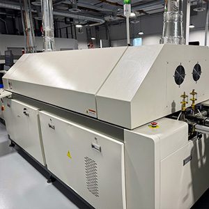
Heating Mode
|
Hot Air Forced Convection
|
|
|
Heated Tunnel Length
|
1910 mm (75")
|
|
|
Temp Control
|
PID (Proportional-Integral-Differential) & SSR
|
|
|
Temperature Range
|
Ambient - 300°C
|
|
|
Precision of Temp Control
|
±1° C
|
|
|
Delta T
|
±2° C
|
|
Certifications & Compliance
- DLA Lab Qualified MIL-STD-883
- ISO 9001:2015 / AS9100:2016
- IPC-A-610, IPC J-STD-001
- ANSI/ESD S20.20 and JESD625 compliance
- Component Traceability & Quality Assurance
- Class 0A ESD certified workstation
Discuss Your CCA Project with Spirit's Technical Team
Contact our seasoned team of engineers, each with over 30 years of experience, to discuss how we can optimize your circuit card assembly, streamline your manufacturing process, and accelerate your time to market through expert consultation and proven solutions.
"*" indicates required fields
Strategic Advantages
Spirit’s comprehensive circuit card assembly (CCA) workflow transforms the traditional multi-vendor process into a streamlined, single-source solution. Instead of managing multiple suppliers, audits, and shipping risks, our AS9100-certified facility handles everything from component procurement and inspection to final system testing and delivery—reducing costs, eliminating handling risks, and accelerating time-to-market while maintaining complete traceability and counterfeit prevention standards.