
Wafer Testing
Overview
Wafer test and sort is the step between front-end fabrication and everything that follows — packaging, assembly, and final qualification — where each die on a wafer is probed and measured before any of it is diced, since process variation across a wafer means die from the same design can still differ in speed, leakage, or basic pass/fail status, and catching that on an intact wafer is far cheaper than discovering it after packaging. Probe testing collects that data die by die through direct contact with each die’s bond pads, capturing functional and parametric (AC/DC) performance that then drives binning — sorting die into performance tiers so each one is matched to the application it’s actually suited for, which matters most in die stacking and multi-chip designs where “Known Good Die” status has to be verified before assembly rather than discovered after it. For mission-critical and harsh-environment applications, that testing typically runs across multiple temperatures rather than a single condition, since military, aerospace, and space deployments rarely operate at a stable room temperature. Below are the specific wafer test capabilities and wire bonding processes Spirit supports as part of that post-foundry flow.
Wafer Test & Sort
Probe Testing
Wafer-level probe testing applies a programmed test pattern to each die on the wafer to collect data about the electrical circuit. Spirit offers a vast array of electrical tests to meet application-specific data needs depending on the wafer complexity. Our process is cost-effective based on die size, number of touch downs and performance to maximize the rate of return and optimize test coverage to the data sheet.
- Purpose: Determine each die’s functional and parametric quality before dicing.
- Condition: Performed on fully fabricated wafers with intact die and accessible bond pads.
- Effect: Identifies pass/fail die and captures key electrical data to avoid packaging defective units.
Sort & Bin
Wafer probe testing determines the reliability and performance limits of each die on the wafer. This data allows you to sort die into performance ranges, optimizing each die’s performance in application. This is especially useful for die stacking and multi-chip designs. Binning reduces low-lot yields, production cost and rework.
- Purpose: Sort die into performance tiers aligned with product requirements.
- Condition: Requires complete probe data and predefined grading criteria.
- Effect: Maximizes product value by matching each die to the optimal performance category.
Three Temp Test
Electrical testing at three temperatures covers additional test parameters for quality and integrity of the die in harsh-environment or mission-critical applications.
- Purpose: Confirm die reliability across extreme temperature ranges.
- Condition: Used for mission-critical applications needing environmental stress validation.
- Effect: Ensures die meet specifications under harsh conditions and reduces field failure risk.
Wafer Test Capabilities
- Wafer Speed Binning
- Wafer Temperature Binning
- Wafer “in family” data segregation
- Known Good Die
- Waffle/Gel Pack sorting
- Function Tests
- AC parameters
- DC parameters
- Application specific I/O test
- Customer configured testing
- Data sheet verification
- Anti-counterfeit validation
Data Collection & Analysis
- Purpose: Gather and interpret test data to support sorting and yield improvement.
- Condition: Completed after probe testing with results mapped to die locations.
- Effect: Enables performance-based binning and detection of wafer-level process issues.
Known Good Die (KGD) Verification
- Purpose: Validate die reliability before use in advanced or high-value packaging.
- Condition: Applies to die destined for complex integration requiring enhanced testing.
- Effect: Prevents defective die from entering advanced assemblies and improves final yield.
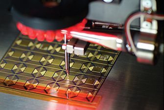
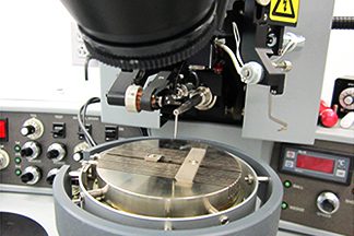
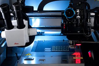
Wire Bonding
Wire bonding is a key manufacturing process for microelectronics and MEMS sensor products. The core wire bonding capabilities and expertise at Spirit Electronics support process development, testing, and manufacturing of sub-assemblies designed by our customers. Wire bonding processes are flexible and robust, allowing our customers to quickly realize a microelectronic package assembly solution for their products. For additional information you can contact us to discuss your wire bonding needs.
- Purpose: Form electrical connections between the die and package using wire interconnects.
- Condition: Conducted after dicing on die that passed testing and align with package design.
- Effect: Provides reliable electrical pathways and supports a wide range of packaging formats.
Fine Gauge Wire/Ribbon Bonding Specifications
|
______________________________________________________________________________________________________________________________________________________________________________________________________________________________________________________________________________________________________________________________________________________________________________________________________________________________________________________________________________________________________________________________________________________________________________________________________________________________
|
______________________________________________________________________________________________________________________________________________________________________________________________________________________________________________________________________________________________________________________________________________________________________________________________________________________________________________________________________________________________________________________________________________________________________________________________________________________________
|
______________________________________________________________________________________________________________________________________________________________________________________________________________________________________________________________________________________________________________________________________________________________________________________________________________________________________________________________________________________________________________________________________________________________________________________________________________________________
|
|---|---|---|
|
Wire diameters
|
17.5µm to 50µm (0.7 to 2.0 mil)
|
|
|
Ribbon
|
6x35µm to 25x250µm (0.25x1.4 mil to 1x10 mil)
|
|
|
Wire and ribbon materials
|
Aluminum, Gold
|
|
|
Pitch Capability
|
Fine pitch is available
|
|
|
Bond area
|
305mm x 410mm (12.3” x 16.14”)
|
|
|
Accuracy
|
1um at 3 sigma
|
|
|
Speed
|
Up to 6 wires/second
|
|
|
Loop Length
|
70 µm up to 20 mm, depending on wire diameter
|
|
|
Various loop form functions
|
Constant wire length
|
|
|
Constant loop height
|
||
|
Individual loop shapes
|
||
Gold Ball Bonding Specifications
|
______________________________________________________________________________________________________________________________________________________________________________________________________________________________________________________________________________________________________________________________________________________________________________________________________________________________________________________________________________________________________________________________________________________________________________________________________________________________
|
______________________________________________________________________________________________________________________________________________________________________________________________________________________________________________________________________________________________________________________________________________________________________________________________________________________________________________________________________________________________________________________________________________________________________________________________________________________________
|
______________________________________________________________________________________________________________________________________________________________________________________________________________________________________________________________________________________________________________________________________________________________________________________________________________________________________________________________________________________________________________________________________________________________________________________________________________________________
|
|---|---|---|
|
Wire diameters
|
15 to 50µm (0.6 to 2.0 mil)
|
|
|
Wire materials
|
Gold
|
|
|
Fine pitch capability
|
40µm
|
|
|
Minimum loop height
|
100µm (standard and worked loops)
|
|
|
Bond area
|
56mm x 80mm
|
|
|
Accuracy
|
+/- 2.0µm
|
|
|
Wire Bonding Speed
|
Up to 15 bonds/second including programmable looping
|
|
|
Looping capability
|
Standard and worked (BGA1-BGA3, Spider, J Wire, CSB)
|
|
|
SSB Capability
|
Stand-off Stitch bond (SSB) capable
|
|
|
Stud Bumping Capability
|
Stud bumping
|
|
|
Wire material
|
Gold
|
|
|
Stud Bumping Speed
|
Up to 30 bumps/second including programmable smoothing
|
|
Heavy Gauge Wire/Ribbon Bonding Specifications
|
______________________________________________________________________________________________________________________________________________________________________________________________________________________________________________________________________________________________________________________________________________________________________________________________________________________________________________________________________________________________________________________________________________________________________________________________________________________________
|
______________________________________________________________________________________________________________________________________________________________________________________________________________________________________________________________________________________________________________________________________________________________________________________________________________________________________________________________________________________________________________________________________________________________________________________________________________________________
|
______________________________________________________________________________________________________________________________________________________________________________________________________________________________________________________________________________________________________________________________________________________________________________________________________________________________________________________________________________________________________________________________________________________________________________________________________________________________
|
|---|---|---|
|
Wire diameters
|
100µm to 500µm (4 to 20 mil)
|
|
|
Ribbon
|
0.075x0.75mm to 0.4mm x 2mm (3x30 mil to 16x80 mil)
|
|
|
Wire and ribbon materials
|
Aluminum
|
|
|
Bond area
|
300mm x 500mm (13.8” x 19.7”)
|
|
|
Accuracy
|
2µm at 3 sigma
|
|
|
Speed
|
Up to 3 wires/sec
|
|
Failure Protection
Products testing outside of specifications or standards pose a failure risk. Improperly leaded finishes can result in whiskering over time.
If your product fails analysis, you can take immediate action to refinish leads, or in the case of failed connection mapping, disqualify an entire lot. Ask us about our testing warranty protection to prevent failures from impacting cost and production time.
Discuss Your Project with Spirit's Technical Team
Spirit can provide complete process development from prototyping through launch. Contact our seasoned team of engineers to discuss your next project.