
Assembly
Microelectronic Sub-Assembly
Precision Manufacturing
Our microelectronic assembly and packaging capabilities take bare die through to packaged, protected, ready-to-integrate subsystems. Precision die attach, wire and ribbon bonding, and encapsulation and dispensing run on production-grade automated equipment in a controlled environment, supporting formats from single-die carriers to multi-die System-in-Package modules. Bonding profiles and sealing methods are matched to each device’s substrate and reliability requirements.

DIE ATTACH
- Die Attach
- Solder Reflow
- Vacuum Solder Reflow
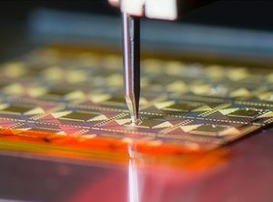
WIRE BONDING
- Fine Gauge Wire / Ribbon Bonding
- Gold Ball Bonding

HEAVY GAUGE WIRE BONDING
- Heavy Gauge Wire / Ribbon Bonding
- Hesse Bondjet Bj939 Heavy Gauge Wire/Ribbon Bonder
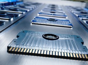
ENCAPSULATION & DISPENSING
- Adhesive Dispense
- Lid Seal
- Parylene Coating
- Near-Hermetic Sealing
Die Attach

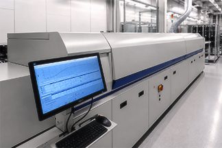

Die Attach Overview
Die attach is a critical step in the packaging of microsystems and MEMS sensors that can impact other packaging and assembly processes. For example, accuracy and repeatability requirements for die placement and die height can affect other package assembly processes such as wire bonding as well as the adhesive and encapsulation materials used. The die attach capabilities and expertise at Spirit Electronics support the process development, testing, and manufacturing of sub-assemblies designed by our customers allowing them to quickly realize a microelectronic package assembly solution for their products. For additional information you can call or send us an email to discuss your die attach needs.
Die Attach Specifications
|
______________________________________________________________________________________________________________________________________________________________________________________________________________________________________________________________________________________________________________________________________________________________________________________________________________________________________________________________________________________________________________________________________________________________________________________________________________________________
|
______________________________________________________________________________________________________________________________________________________________________________________________________________________________________________________________________________________________________________________________________________________________________________________________________________________________________________________________________________________________________________________________________________________________________________________________________________________________
|
______________________________________________________________________________________________________________________________________________________________________________________________________________________________________________________________________________________________________________________________________________________________________________________________________________________________________________________________________________________________________________________________________________________________________________________________________________________________
|
|---|---|---|
|
Die Attach Methods
|
Epoxy die attach, flip chip, sintering, eutectic attach, multi-chip module
|
|
|
X/Y placement accuracy
|
±7μm @ 3 sigma
|
|
|
Theta placement accuracy
|
±0.15° @ 3 sigma
|
|
|
Die thickness
|
Down to 20μm
|
|
|
Speed
|
Up to 7,000 units per hour
|
|
|
Material presentations
|
Grip ring and film frame (for wafers up to 300mm), waffle pack, Gel-Pak
|
|
|
Substrates
|
FR4, ceramic, BGA, flex, boat, lead-frame, waffle pack, Gel-Pak, JEDEC tray
|
|
Vacuum Solder Reflow Specifications
- Flux-less and void-free soldering
Hermetic package sealing
Controlled cooling in N2 gas
Automatic control of vacuum and gas backfill pressure
Vacuum minimum 50mTorr
Chamber gas pressure maximum 40psig
Operating temperature range of 100 to 500°C
Uniform heat distribution supplied by single sheet graphite heating element
Automatic control of heating and cooling ramp rates
Formic acid capable
12.0×12.0 inch thermal working area
Solder Reflow Specifications
|
______________________________________________________________________________________________________________________________________________________________________________________________________________________________________________________________________________________________________________________________________________________________________________________________________________________________________________________________________________________________________________________________________________________________________________________________________________________________
|
______________________________________________________________________________________________________________________________________________________________________________________________________________________________________________________________________________________________________________________________________________________________________________________________________________________________________________________________________________________________________________________________________________________________________________________________________________________________
|
______________________________________________________________________________________________________________________________________________________________________________________________________________________________________________________________________________________________________________________________________________________________________________________________________________________________________________________________________________________________________________________________________________________________________________________________________________________________
|
|---|---|---|
|
Accommodations
|
18” wide boards and substrates and maximum clearance of 2.2”
|
|
|
Tunnel length
|
105” includes 9 heating zones each with independently controlled top and bottom heaters
|
|
|
Maximum temperature
|
450 °C with PID temperature control ± 1°C per zone and ± 3° cross-belt temperature tolerance
|
|
|
Internal controlled cooling zone
|
30” length includes 3 cooling zones with top and bottom cooling
|
|
|
Atmosphere Control
|
Balanced flow of air or nitrogen capable of producing controlled atmospheres less than 25 ppm O2
|
|
|
Process Monitoring & Data Logging
|
CPK & SPC data and alarm logging with timed download and profile printout capability
|
|
Wire Bonding
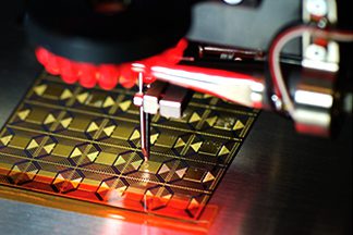
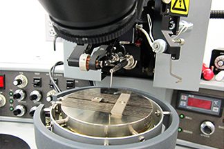
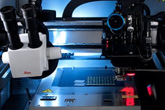
Wire Bonding Overview
Wire bonding is a key manufacturing process for microelectronics and MEMS sensor products. The core wire bonding capabilities and expertise at Spirit Electronics support process development, testing, and manufacturing of sub-assemblies designed by our customers. Wire bonding processes are flexible and robust, allowing our customers to quickly realize a microelectronic package assembly solution for their products. For additional information you can call or send us an email to discuss your wire bonding needs.
Fine Gauge Wire/Ribbon Bonding Specifications
|
______________________________________________________________________________________________________________________________________________________________________________________________________________________________________________________________________________________________________________________________________________________________________________________________________________________________________________________________________________________________________________________________________________________________________________________________________________________________
|
______________________________________________________________________________________________________________________________________________________________________________________________________________________________________________________________________________________________________________________________________________________________________________________________________________________________________________________________________________________________________________________________________________________________________________________________________________________________
|
______________________________________________________________________________________________________________________________________________________________________________________________________________________________________________________________________________________________________________________________________________________________________________________________________________________________________________________________________________________________________________________________________________________________________________________________________________________________
|
|---|---|---|
|
Wire diameters
|
17.5µm to 50µm (0.7 to 2.0 mil)
|
|
|
Ribbon
|
6x35µm to 25x250µm (0.25x1.4 mil to 1x10 mil)
|
|
|
Wire and ribbon materials
|
Aluminum, Gold
|
|
|
Pitch Capability
|
Fine pitch is available
|
|
|
Bond area
|
305mm x 410mm (12.3” x 16.14”)
|
|
|
Accuracy
|
1um at 3 sigma
|
|
|
Speed
|
Up to 6 wires/second
|
|
|
Loop Length
|
70 µm up to 20 mm, depending on wire diameter
|
|
|
Various loop form functions
|
Constant wire length
|
|
|
Constant loop height
|
||
|
Individual loop shapes
|
||
Gold Ball Bonding Specifications
|
______________________________________________________________________________________________________________________________________________________________________________________________________________________________________________________________________________________________________________________________________________________________________________________________________________________________________________________________________________________________________________________________________________________________________________________________________________________________
|
______________________________________________________________________________________________________________________________________________________________________________________________________________________________________________________________________________________________________________________________________________________________________________________________________________________________________________________________________________________________________________________________________________________________________________________________________________________________
|
______________________________________________________________________________________________________________________________________________________________________________________________________________________________________________________________________________________________________________________________________________________________________________________________________________________________________________________________________________________________________________________________________________________________________________________________________________________________
|
|---|---|---|
|
Wire diameters
|
15 to 50µm (0.6 to 2.0 mil)
|
|
|
Wire materials
|
Gold
|
|
|
Fine pitch capability
|
40µm
|
|
|
Minimum loop height
|
100µm (standard and worked loops)
|
|
|
Bond area
|
56mm x 80mm
|
|
|
Accuracy
|
+/- 2.0µm
|
|
|
Wire Bonding Speed
|
Up to 15 bonds/second including programmable looping
|
|
|
Looping capability
|
Standard and worked (BGA1-BGA3, Spider, J Wire, CSB)
|
|
|
SSB Capability
|
Stand-off Stitch bond (SSB) capable
|
|
|
Stud Bumping Capability
|
Stud bumping
|
|
|
Wire material
|
Gold
|
|
|
Stud Bumping Speed
|
Up to 30 bumps/second including programmable smoothing
|
|
Heavy Gauge Wire/Ribbon Bonding Specifications
|
______________________________________________________________________________________________________________________________________________________________________________________________________________________________________________________________________________________________________________________________________________________________________________________________________________________________________________________________________________________________________________________________________________________________________________________________________________________________
|
______________________________________________________________________________________________________________________________________________________________________________________________________________________________________________________________________________________________________________________________________________________________________________________________________________________________________________________________________________________________________________________________________________________________________________________________________________________________
|
______________________________________________________________________________________________________________________________________________________________________________________________________________________________________________________________________________________________________________________________________________________________________________________________________________________________________________________________________________________________________________________________________________________________________________________________________________________________
|
|---|---|---|
|
Wire diameters
|
100µm to 500µm (4 to 20 mil)
|
|
|
Ribbon
|
0.075x0.75mm to 0.4mm x 2mm (3x30 mil to 16x80 mil)
|
|
|
Wire and ribbon materials
|
Aluminum
|
|
|
Bond area
|
300mm x 500mm (13.8” x 19.7”)
|
|
|
Accuracy
|
2µm at 3 sigma
|
|
|
Speed
|
Up to 3 wires/sec
|
|
Heavy Gauge Wire and Ribbon Bonding
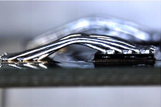
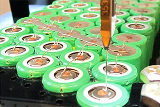
Overview
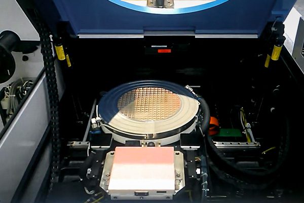
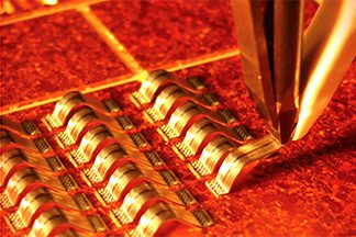
Wire bonding is a commonly used process to create low-cost and reliable electrical interconnects between semiconductor components and mechanical assemblies. Wire bonding is generally considered the most cost-effective and flexible interconnect technology for microelectronic assembly. It is used to manufacture the vast majority of fully packaged semiconductor products.
Hesse Bondjet BJ939 Heavy Gauge Wire/Ribbon Bonding Specifications
|
______________________________________________________________________________________________________________________________________________________________________________________________________________________________________________________________________________________________________________________________________________________________________________________________________________________________________________________________________________________________________________________________________________________________________________________________________________________________
|
______________________________________________________________________________________________________________________________________________________________________________________________________________________________________________________________________________________________________________________________________________________________________________________________________________________________________________________________________________________________________________________________________________________________________________________________________________________________
|
______________________________________________________________________________________________________________________________________________________________________________________________________________________________________________________________________________________________________________________________________________________________________________________________________________________________________________________________________________________________________________________________________________________________________________________________________________________________
|
|---|---|---|
|
Wire diameters
|
100µm to 500µm (4 to 20 mil)
|
|
|
Ribbon
|
0.075mm x 0.75mm to 0.3mm x 2mm
|
|
|
Wire and ribbon material
|
Aluminum
|
|
|
Working area
|
X: 350 mm; Y: 560 mm; Z: 70 mm (13.8” x 20.0” x 2.76”)
|
|
|
Accuracy
|
2µm at 3 sigma
|
|
|
Speed
|
Up to 3 wires/sec
|
|
Key Insights on Heavy Gauge Wire and Ribbon Bonding
FIXTURING – A custom fixture must be designed to securely hold the parts before wire bonding can begin.
PROCESS TOOLING – The assembly must be designed to accommodate the wire bond process tooling.
PAD SIZE – The wire bond interconnect pads must be properly sized to accommodate the wire bonds.
METALLIZATION – The metallization of the wire bond pad needs to be designed to be compatible with the chosen interconnect bond wire that can withstand the environmental and mechanical conditions of the end application.
STRUCTURAL SUPPORT – The assembly must be designed to fully support the structure beneath the wire bonds.
Technical Resources
- Product Design for Wire-Bondability
- Developing Robust Interconnects for Microelectronic Assemblies
- Lessons Learned for Wire Bond Interconnect Process Success
- Destructive Wire Bond Testing for Development and Production
- Destructive Wire Bond Shear Testing and Its Purpose
- Destructive Wire Bond Pull Testing and Its Purpose
- Wire Bonding Services Data Sheet
Encapsulation and Dispensing
Encapsulation and Dispensing Overview
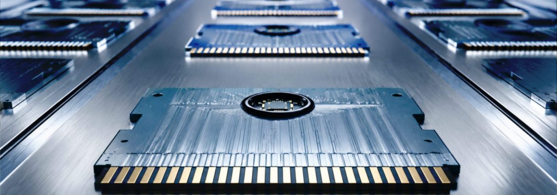
Encapsulation of microsystems is a sophisticated process requiring understanding of the encapsulant materials and their interactions with die surfaces, package substrates and their related processes, as well as the physical environment in which the packaged device will be exposed. The encapsulation capabilities and expertise at Spirit Electronics support the process development, testing, and manufacturing of sub-assemblies designed by our customers allowing them to quickly realize a microelectronic package assembly solution for their products. For additional information you can call or send us an email to discuss your encapsulation needs.
Adhesive Dispense Specifications
• Dam and fill
• Glob top
• Potting
• Epoxies, heat cures, UV cures, thixotropic adhesives
• Time/pressure dispense, auger dispense, and jetted dispense
• Weight controlled dispensing
• X-Y repeatability: ±25µm
• Z-axis repeatability: ±25µm
• X -Y Travel: 525 x 525 mm (20.7 x 20.7 in.)
• Z Travel: 75 mm (2.95 in.) maximum
Lid Seal Specifications
• Solder, epoxy, tape
• Hermetic and non-hermetic
• TO headers, DIP packages, open cavity plastic packages, ceramic packages
Parylene Coating Specifications
• Chamber Size 12 inch dia. X 12 inch high (8.5”/31.5cm dia. X 11.19”/28.4cm H, useable size)
• Dimer Capacity 125 grams
• Cold Trap using Mechanical Chiller
• Deposits Parylene type C at 0.0002” per hour
• Deposits Parylene type N at 0.00003” per hour
Discuss Your Project with Spirit's Technical Team
Spirit can provide complete process development from prototyping through launch. Contact our seasoned team of engineers to discuss your next project.